Thank you for visiting nature.com. You are using a browser version with limited support for CSS. To obtain
the best experience, we recommend you use a more up to date browser (or turn off compatibility mode in
Internet Explorer). In the meantime, to ensure continued support, we are displaying the site without styles
and JavaScript.
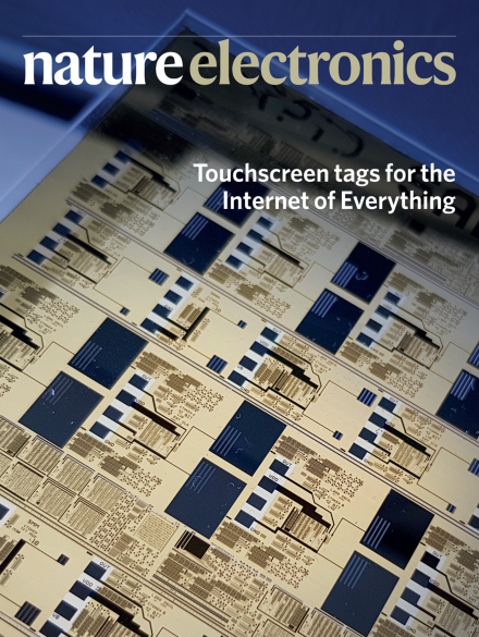
Radio-frequency identification tags built from thin-film transistor technology can communicate with commercial capacitive touchscreens, allowing these ubiquitous screens to be used as reader interfaces. The tags can also be powered by thin-film photovoltaic cells that convert light from the touchscreens. The cover shows a photograph of the capacitive tags fabricated on a plastic substrate.
A slanted tri-gate geometry improves electric field management in multi-channel AlGaN/GaN power transistors leading to higher breakdown voltage and lower on-resistance.
With the help of extreme-ultraviolet lithography and high-mobility-channel fin field-effect transistors, the Taiwan Semiconductor Manufacturing Company deliver their latest CMOS platform for use in mobile and high-performance computing applications.
Gate dielectrics with an equivalent oxide thickness of only one nanometre can be grown on two-dimensional semiconductors with the help of a monolayer molecular crystal.
Using a monolayer molecular crystal as a seeding layer, hafnium oxide dielectrics with an equivalent oxide thickness of only 1 nm can be deposited on graphene, molybdenum disulfide and tungsten diselenide.
The absorption profile of photodetectors based on silicon can be extended into the near- and shortwave-infrared regions by taking advantage of optical resonance effects.
A ferroelectric semiconductor field-effect transistor, which uses the two-dimensional ferroelectric semiconductor α-In2Se3 as a channel material, could offer enhanced capabilities compared with conventional ferroelectric field-effect transistors in non-volatile memory applications.
Thin-film transistors with a high electron mobility and operational stability can be fabricated from solution-processed multilayer channels composed of ultrathin layers of indium oxide, zinc oxide nanoparticles, ozone-treated polystyrene and compact zinc oxide.
A floating-gate memristive device fabricated in a commercial 180 nm CMOS process can be integrated into a selector-free memristive array and used to demonstrate basic neuromorphic applications.
Commercial touchscreens can serve as a reader interface for capacitive coupled data transfer using identification tags that are fabricated with thin-film transistor technology and powered by thin-film photovoltaic cells that convert light from the touchscreens.