Thank you for visiting nature.com. You are using a browser version with limited support for CSS. To obtain
the best experience, we recommend you use a more up to date browser (or turn off compatibility mode in
Internet Explorer). In the meantime, to ensure continued support, we are displaying the site without styles
and JavaScript.
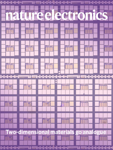
Operational amplifiers can be fabricated from two-dimensional molybdenum disulfide field-effect transistors and used to create analogue feedback circuits such as inverting amplifiers, integrators, log amplifiers and transimpedance amplifiers. The cover shows an optical microscopy image of a chip containing these operational amplifiers (each with a footprint of around 0.04 mm2), as well as test transistors.
Two-dimensional materials could first find widespread commercial application in analogue electronics, rather than as a replacement for silicon in digital devices.
A van der Waals ferroelectric tunnel junction with asymmetric metal and graphene contacts exhibits a high resistance ratio between on and off states, and could be of value in the development of low-power computing.
The two-dimensional semiconductor Bi2O2Se can be oxidized to create an atomically thin layer of Bi2SeO5 that can be used as the insulator in scaled field-effect transistors.
Monolayers of boron nitride can be used to build high-performance radio-frequency switches that can operate at the frequencies required for 5G and the communication systems beyond it.
This Review Article examines the potential of spintronics in four key areas of application —memories, sensors, microwave devices, and logic devices — and discusses the challenges that need be addressed in order to integrate spintronic materials and functionalities into mainstream microelectronic platforms.
Electrostatic gating can be used to modulate the magnetic anisotropy of chromium germanium telluride, a layered ferromagnetic semiconductor, and increase its Curie temperature to 200 K.
A ferroelectric tunnel junction that uses copper indium thiophosphate as the ferroelectric barrier, and graphene and chromium as asymmetric contacts, can offer a high resistance ratio between on and off states.
An atomically thin high-κ gate dielectric of Bi2SeO5 can be formed via layer-by-layer oxidization of an underlying two-dimensional semiconductor, allowing high-performance field-effect transistors and inverters to be fabricated.
Resistive switching in atomically thin sheets of hexagonal boron nitride can be used to create analogue switches for applications in communication systems across radio, 5G and terahertz frequencies.
An operational amplifier that uses the two-dimensional semiconductor molybdenum disulfide as the active material can be used to create complex analogue circuits, including inverters, integrators and amplifiers.
Using a solution-based deposition technique, carbon nanotube field-effect transistors can be fabricated in a commercial silicon manufacturing facility and a high-volume commercial foundry, demonstrating uniform and reproducible transistor fabrication across industry-standard 200 mm wafers.