Thank you for visiting nature.com. You are using a browser version with limited support for CSS. To obtain
the best experience, we recommend you use a more up to date browser (or turn off compatibility mode in
Internet Explorer). In the meantime, to ensure continued support, we are displaying the site without styles
and JavaScript.
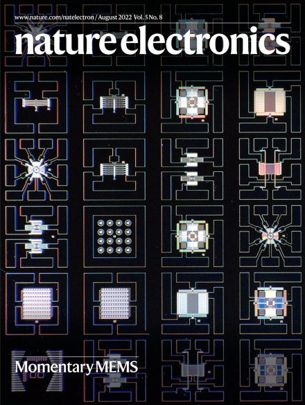
Microelectromechanical systems (MEMS) that are based on water-soluble materials can resorb into the environment to eliminate waste, or into the body to avoid the need for surgical extraction, after a targeted lifetime. The photograph on the cover shows various ecoresorbable and bioresorbable MEMS devices supported within a single die.
The development of microelectromechanical systems that decompose after use expands the toolbox of transient electronics, a technology that could help reduce electronic waste.
Silicon-based dual-gate photodiodes with electrostatically controlled photocurrents can be used to create imaging systems that can compute incoming visual data.
Laser-assisted chemical reactions have been used to write reversible ultra-high-density doping patterns in graphene for optoelectronic applications. The approach used two laser beams with specific photon energies and geometric configurations to enable local doping with a high dopant coverage ratio on graphene, while preserving the electronic properties of the surface.
Microelectromechanical systems that can disintegrate and degrade after a targeted lifetime are demonstrated alongside bioresorbable encapsulating materials and deployment strategies that offer safe biointegration of such devices. These devices have the potential to reduce electronic waste and help create temporary biomedical implants.
Lattice distortions induced by ripples in two-dimensional molybdenum disulfide can reduce electron–phonon scattering, leading to improved charge carrier mobility and enhanced transistor performance.
Vanadium diselenide van der Waals contacts made with a controlled crack formation process can be used to fabricate tungsten diselenide transistors with channel lengths of less than 100 nm, on-state current densities of up to 1.7 mA μm–1 and on-state resistances down to 0.50 kΩ μm.
Two laser beams with different energies and configurations can be used to reversibly dope graphene via chlorination and chlorine removal, allowing rewritable graphene photodetectors to be fabricated.
Solution-processed lead–tin binary perovskite photodetectors that have an external quantum efficiency of 85% at 850 nm, dark current below 10–8 A cm–2 and response time faster than 100 ps can be used in light detection and ranging applications, resolving sub-millimetre distances with a typical 50 µm standard deviation.
A network of dual-gate silicon p–i–n photodiodes, which are compatible with complementary metal–oxide–semiconductor fabrication processes, can perform in-sensor image processing by being electrically programmed into convolutional filters.
Transient micro-electromechanical system (MEMS) devices that are based on water-soluble material platforms can provide safe implants for biointegrated systems.